


Please enter the answer below before you can view the full text.
8+6=
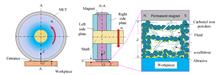
To achieve high-efficiency and low-defect machining of fused silica optics, the material removal characteristics and surface quality formation mechanism based on magnetically assisted polishing technology were studied. Magnetic polishing fluid with different degrees of polishing clearance and different volume ratios of iron powders was used to conduct magnetically assisted polishing of lapped fused silica optics. The material removal rate, profile of polished spots, surface roughness, and transmittance of samples were evaluated, and the effects of the processing parameters on processing efficiency and surface quality were determined by combining a spatial magnetic flux intensity simulation and polishing pressure analysis. Results show that the material depth removal rate increases as a power function with the magnetic flux intensity and rises significantly with the volume ratio of iron powders in the polishing fluid. In addition, polishing fluid with a low spatial magnetic field intensity and low volume ratio of iron powders can facilitate material removal in the elastic domain, resulting in a smooth surface. A small polishing clearance of 0.5 mm and high iron powder volume ratio of 14.18% in the polishing fluid can obtain maximum depth removal and volume removal rates of 0.439 2 μm/min and 1.49 × 10⁻⁴ mm3/min, respectively. A large polishing gap of 1.5 mm and a low volume ratio of iron powders of 9.93% generates a smooth surface with Ra roughness as low as 8.1 nm.
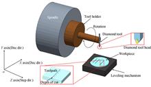
In the processing of infrared optical microstructured surfaces, the hard, brittle, and difficult-to-machine properties of infrared optical materials and the complex geometric properties of microstructured surfaces lead to uneven and brittle fractures in the processed microstructured surfaces and reduce the face shape accuracy. Small feeds are now commonly used to suppress surface fragmentation but are inefficient. To achieve efficient, high-precision, and low-damage machining of infrared optical microstructured surfaces, an ultra-precise adaptive flying cutting method was proposed and experimentally validated in this study. First, based on the kinematic characteristics of flying cutting, a flying cutting plasticity machining model was established. Second, based on the principle whereby the maximum chip thickness was always less than the brittle-plastic transition threshold, an iterative algorithm was used to plan a tool trajectory with dynamically varying feed rates based on the local morphological characteristics of the microstructured surface. Finally, the effectiveness of the proposed adaptive flying cutting method was verified by comparing it with the conventional flying cutting method in experiments. Experiments show that microgrooves are successfully machined without brittle fracture on single-crystal silicon materials and that a surface roughness of 18 nm is achieved. Compared with conventional flying tool cutting methods, the proposed ultra-precision adaptive flying cutting method avoids brittle breakage without reducing feed rates and achieves 2.5 times the machining efficiency of conventional methods.
The modulation of the phase wavefront of geometric phase metasurface lenses does not depend on the cumulative phase of the propagation process. However, it affects the local polarization state through the space-variant unit structure and introduces the conjugate additional phase that focuses the incident beam, which differs from the characteristics of traditional refractive lenses. For interference lithography fabrication of geometric phase metalens structures, an optical Fourier transform system modulated by a space-variant phase element is proposed in this study. Subsequently, the orientation and frequency-variant micron structures were prepared using interference lithography. Based on the Fourier transform theory of optical lens and geometric propagation principle of light diffraction, the influence of light field on image plane based on the inserted sub-phase-elements with different frequencies, orientations, and relative positions was analyzed. Therefore, a method was proposed for multi-interference light fields with sectionalized modulation of space-variant phase elements on incident light. Moreover, the preparation of orientation and period-variant micron structure based on multiple simultaneously generated light fields were illustrated. Accordingly, utilizing the designed and fabricated space-variant phase element, interference light fields with circle and ring distributions were simultaneously generated. The experimental results demonstrate that space-variant grating structures with orientations of 0°, 125°, and 235°, periods of 7.22, 6.51, and 5.78 μm, and micron pattern structure with radius of 1 892 μm can be obtained simultaneously. The proposed optical system is simple and easy to be combined with a projection exposure system and has great potential for manufacturing geometric phase metalens devices based on a space-variant micro-nano unit cell.
The metalens constructed by the micro-nano structure array is not only small and lightweight, but also has a multi-functional design that can be realized through a composite structure. The existing metalens diameters are generally in the order of micrometers. For a metalens such as a centimeter-level diameter, the number of micro-nano structure units contained in it can reach billions. If these massive micro-nano structures are drawn by modeling them sequentially, the layout file will inevitably be too large, such that the drawing time is so long that the layout cannot be opened. To solve this problem, this study proposes a circular layout metalens design method based on the layout design software L-Edit. This method uses binary coding to divide the metalens into blocks to compress the layout file. Numerical simulation results show that the designed metalens achieves sub-wavelength focusing. For the 50 mm diameter metalens, the layout file size obtained using the proposed layout drawing method is 176 MB. This is much smaller than the layout file size (3.70 TB) generated by the one-by-one modeling and drawing method. This study proves that an efficient compression of massive data of a large-aperture metalens in the layout design ensures the manufacturability of the design of large-aperture metalens elements.
The key fabrication technology for diffractive optical elements (DOE) was systematically investigated from the following four aspects: graphic data processing, advanced lithography, pattern transfer, and large-area integration with high reliability. Based on the standard CMOS process, a complete set of manufacturing technologies for DOE with high precision, multi-functionality (high fidelity, high aspect ratio, high surface flatness, multiple substrates, etc.), and large area was proposed. A data processing system with precision greater than 2 nm is developed for complex pattern lithography. Moreover, a hybrid lithography method was proposed and two types of basic pattern transfer techniques and four different processes are established, including additive processes (lift-off and electroplating) and subtractive processes (drying etching and low-temperature metal assisted chemical etching). Importantly, we demonstrate the pattern generation from micron to sub-10 nm scale, pattern transfer of 25 nm gold structures with aspect ratio of 12∶1, and 30 nm Al2O3 nanotubes with aspect ratio up to 500∶1. Based on various substrates, including fused quartz, multilayer film, SiC self-supporting membrane, and wafer with high surface flatness, various large-area DOEs are integrated. The maximum area is 142 mm×142 mm, the maximum self-supporting aperture is 70 mm, and the highest surface flatness is 0.03λ peak to valley. Our proposed framework can meet the manufacturing requirements of various DOEs, covering the spectral bands ranging from visible light to hard X-rays. Various DOEs are used in four major optical projects, including advanced lithography, synchrotron radiation, laser fusion, and X-ray astronomy, as well as more than 1 000 domestic and foreign universities, scientific research institutes, and high-tech enterprises.
Multifunctional and highly integrated all-fiber devices has promoted the development of lab-on-fiber technology. The rapid progress in the manufacturing technology has opened up a new avenue for the multifunctional plug-and-play fiber-optic platform. Researchers are committed to exploring and optimizing the onboard laboratory preparation technology to show the potential of onboard laboratory components in many application scenarios. First, we review the classification of fiber-on-lab technology and describe the preparation process of nanostructure at the fiber end facet, including physical and chemical processing methods. Then, we discuss the research progress of lab-on-fiber preparation technology based on the metasurface on the fiber end facet and the difficulties in the process of technology development. Finally, we clarify the strategy of constructing multi-functional, highly integrated, and multi-application scenarios of fiber sensing devices. The remarkable achievements of lab-on-fiber technology clearly show that multifunctional, highly integrated all-fiber devices can play a vital role in many scenarios related to physical and biochemical parameter monitoring, particle capture, and light field regulation.